RF communication between Arduino Nanos using nRF24L01
In this tutorial I’ll go through a simple example of how to get two Arduino Nano devices to talk to one another.
Materials
You’ll need the following materials. I’ve posted Amazon links just so that you can see the items, but they can be purchased in a variety of locations.
About the nRF24L01+
The nRF24L01+ is an appealing device to work with because it packs a lot of functionality on-chip as opposed to having to do it all in software. There is still a lot of work to be done in code; but it’s a good balance between simplicity and functionality. It’s also inexpensive.
What follows is a lengthy description of the nRF24L01+ device. If you just want to connect up your devices, then you can skip to the device hookup section.
nRF24L01+ theory of operation
There are several libraries for the nRF24L01 in the public domain that seek to simplify interactions with a variety of MCU’s. While they are fine (and we’ll make use of one here) you should understand how the device works so that when you inevitably branch out from the basic demonstration projects, you know how to achieve what you want. Read the nRF24L01 datasheet. I’ll start out here by reviewing it at a high level.
More than likely you are working with a breakout board for this surface-mount device. So you will concern yourself only with the following pins: Vcc, GND, CE, CSN, IRQ, MISO, MOSI, SCK. For the purposes of this example, we won’t be using the interrupt line IRQ so you can leave it disconnected.
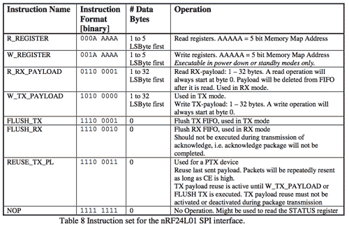
The nRFL01 has a relatively simple instruction set for the SPI interface.
Reading from nRF24L01 registers
The protocol for addressing the transceiver via the SPI instruction set begins by bringing the CSN line from high to low, thus informing the nRFL01 that an instruction is about to be clocked into it. Next you clock in the command byte for the instruction you which to execute, followed by the data relevant to that instruction. Before we talk about how to configure the instructions, we should glance at the register addresses because we will refer to their addresses in the examples. You will find the memory map of the addresses on pages 22-26 of the nRF24L01 datasheet. For our example, let’s assume we want to read the RF_SETUP register. From page 23 of the nRF24L01 datasheet we see that the memory address is 0x06. To read that register, we bring CSN low, send an R_REGISTER instruction encoded with the register address. From Table 8, we see that the format for this instruction is 0b000aaaaa where the 5 bits aaaaa represent the memory address of the register. In this case we would send 0b00000110 (0x06). For this instruction, we expect a single byte return. To get that return we have to clock in a dummy byte on MOSI. Note that every command also returns the STATUS register.
Writing to nRF24L01 registers
The device would be useless if we couldn’t write to any registers, so we should talk about how to do that. Table 8 shows the W_REGISTER command has the following format: 0b001aaaaa where the 5 lower bits represent the address of the register we want to write to. Let’s say we want to set the data rate to 1 Mps and the RF output power to minimum. First let’s take a look at the format for the RF_SETUP register:
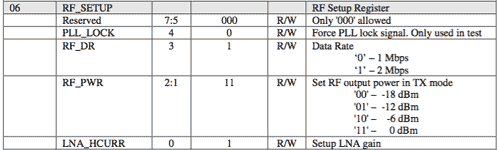
The upper 3 bits are reserved and should be 000. The PLL_LOCK bit is only used in testing. So that leaves us with bits 3:0. Bit 3 RF_DR sets the data rate. Since we want 1 Mbps, that bit gets unset. The next 2 bits set the RF_PWR. Minimum power is 00 for these two bits. The last bit LNA_HCURR sets the low noise amplifier gain. The nRF24L01+ datasheet discusses the LNA gain in more depth. The LNA gain allows the device to reduce the current consumption in receive mode at the expense of some receiver sensitivity. Since we’ll be sufficiently powered, it’s OK to leave that bit unset.
So, the write protocol is to drop CSN and send the W_REGISTER command configured for the address of interest. So, we’ll send 0b00100110 (0x26) followed by 0b00000000 (0x00) to congure it in the way we describe above (1 Mbps, low output power.)
Read receive payload
The next command of interest is the R_RX_PAYLOAD which as the name implies reads a payload of bytes that were received by the device. The command format requires no configuration; it is simply 0b01100001 (0x61.) There is some “choreography” involved in using this command because you must manipulate the CE pin also. How do you know you’ve received a packet? You know a packet has been received when an RX_DR (data ready) interrupt has been triggered. We’ll get to this later but for now, you should know that this interrupt exists as a bit in the STATUS register (yes, the register that we constantly get returned when we send any command.) We can also choose to configure the transceiver to send a hardware interrupt when it receives a package. When a unit is receiving, the CE pin must be high, once you’ve received a package, you have to bring the CE pin low, the send the R_RX_PAYLOAD command as usual. Next, you clock in the same number of dummy bytes as your payload size in order to read out the payload. What happens if you’ve received multiple payloads? The device keeps multiple payloads (3 per pipe) in a first-in, first-out (FIFO) stack. When you’re done receiving, you should clear the RX_DR interrupt and bring the CE pin high again to start receiving.
Write receive payload
To write a payload, we’ll use the W_TX_PAYLOAD. When your device is transmitting, you hold CE low (opposite of read). The “choreography” here is a little different. First we send a W_TX_PAYLOAD (0b10100000 = 0xA0) along with the number of bytes specified by the payload size. Next, we signal a transmit by toggling the CE pin from low to high to low over at least 10 µs. The ТХ_DS interrupt will be set if the packet is sent. Actually, the behaviour is a little more complicated than that. This interrupt actually depends on whether you have auto-acknowledge enabled for the pipe. If you do, then the TX_DS interrupt is only set if you get an ack from the receiver on the pipe. If you are auto-acknowledging on that pipe then, then you also have to look for the MAX_RT flag on the STATUS register to see whether the maximum number of retries has been reached. As with the receiver, there’s also a FIFO transmit stack, so you can stack up to three packets before sending (by toggling CE.)
Flushing the TX and RX stacks
There are two SPI commands that clear the TX and RX FIFO stacks, FLUSH_TX and FLUSH_RX respectively. Neither has has any associated bytes.
NOP command reads STATUS register
There is a NOP (no operation) command that takes no additional bytes and whose only purpose is to read back the STATUS register quickly. It is faster than R_REGISTER because you don’t have to pass the address of the STATUS register.
nRF24L01 registers
Next, I’ll be talking about some of the nRFL01 registers. Since the nRF24L01 datasheet covers everything, we’ll just go over the high points and any gray areas. As always, if you just want to get two Arduinos talking to each other, you can skip to the device hookup section.
Configuration register
The CONFIG register at address 0x00, has a number of useful bits.
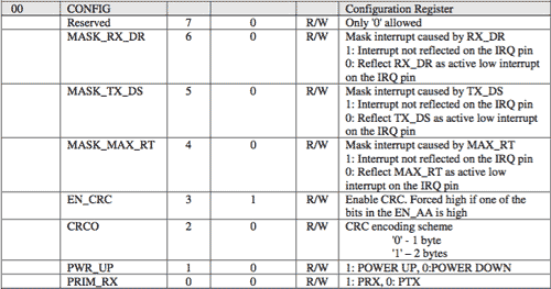
Bits 6,5,4 control how we use the IRQ pin. If we want the RX_DR (packet received) interrupt to show up on the IRQ pin, then we would set the MASK_RX_DR bit. Then it will show up as an active low state on the IRQ pin. Likewise for the MASK_TX_DS interrupt. Remember that the TX_DS flag behaviour depends on whether we’ve enabled auto-acknowledge for the pipe we’re using. The MASK_MAX_RT bit determines whether the MAX_RT state is reflected on the IRQ pin or not. The EN_CRC enables CRC error detection and its default value is 1 (enabled.) You can control power to the transceiver by manipulating the PWR_UP bit. The last bit is the PRIM_RX. If set, your device is a receiver; otherwise it’s a transmitter.
Enable auto-acknowledgment registers
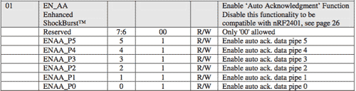
You can enable or disable auto-acknowledgment on any of the 6 data pipes via this register. For the most fault-tolerant system design, you should enable the auto-acknowledgment on the pipes you are using.
Enable RX addresses
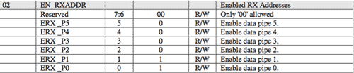
To enable receiving on a given pipe, set its bit in this register.
Set address width register
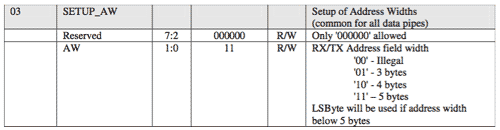
The width of each address across all data pipes, both receive and transmit is set via this register. The width can be configured to be from 3-5 bytes in length and it must be consistent between all devices. Longer is better.
Setup automatic retransmission
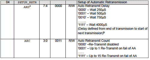
In this register you can set up how many times to retry transmission after an initial failure. The number of tries is setup in the lower 4 ARC bits and can therefore range from 0x00 to 0x0F. If automatic retransmission is enabled, the upper three bits specify the delay in microseconds. Each unit from 0-15 increases the delay by 250 µs.
OBSERVE_TX register
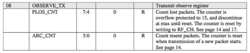
The register is a sort of quality-control register. The upper 4 bits count the number of lost packets and is reset by writing to the the RF_CH register. The lower 4 ARC_CNT bits provide a count of the number of retransmissions. It is reset with each new packet.
Received power detector registers
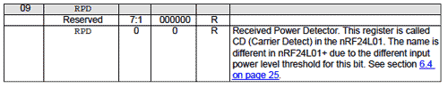
The RPD register was previously called the CD (carrier detect) register on the nRF24L01. Only the lower bit is relevant. It triggers to 1 if the received power is above -64 dBm currently receiving, or zero if less than -64 dBm.
Receive address registers
The receive address registers occupy the memory offsets from 0x0A to 0x0F for data pipes 0-5. They are known by the RX_ADDR_Px where x is 0-5. Note that RX_ADDR_P0 is 40 bits wide with a reset value 0xE7E7E7E7E7. RX_ADDR_P is also 40 bits wide but has a reset value of 0xC2C2C2C2C2. The remaining addresses are only a single byte register because they must differ from the base address only by the LSB, the one that is stored.
Transmit address register
Register TX_ADDR occupies memory address 0x10 and is used only on a primary transmitter PTX device. If you want to use auto-ack, this address must be the same as RX_ADDR_P0.
Receive channel payload widths
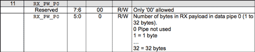
Each of the six data pipes can have its own payload width. The registers that specify these widths all follow the same format as the RX_PW_P0 register depicted about. The occupy memory slots 0x11 to 0x16. Only the lower 6 bits are used and therefore can express numbers from 1-32.
FIFO status register
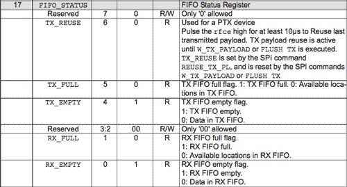
The FIFO status register at 0x17 reports the status of the FIFO receive and transmit stacks along with related information. The TX_REUSE flag is set when a transmit payload has been reused by pulsing the CE high and using the REUSE_TX_PL command. The rest of the bits relate to the current state (empty or full) of the receive and transmit payload stacks.
Status register
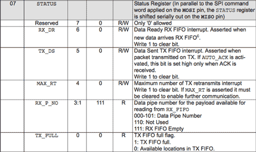
We see a lot of the status register because it gets returned to us, remember, when we clock in a command, whether we ask for it or not. The RX_DR bit is set new data arrives in the receive stack. You can clear this flag by writing a 1 to it. Similarly, the TX_DR bit is set when a packet gets transmitted. If you have enabled AUTO_ACK then this bit gets flipped only when you receive and ACK signal. The MAX_RT flag is set when the maximum number of retransmit retries had been reached. If it gets set, you must reset this flag manually by writing 1 to it. Otherwise you cannot go on transmitting. RX_P_NO these bits reflect the number of the data pipe that has data in the receive FIFO. Finally, the TX_FULL flag is set when the transmit FIFO is full.
nRF24L01+ registers
Some registers are unique to the newer nRF24L01+ device.
DYNPD enable dynamic payload length
The DYNPD register at memory offset 0x1C allows you to enable dynamic payload length on specific data pipes. We will be using fixed payload length in our example.
FEATURE register
The FEATURE register allows you to set features related to dynamic payload length. We’ll leave this to a later discussion since we won’t use this in our example.
Are you finally ready to start connecting everything?
Setting up the devices
Attach the transceiver breakout board to the Arduino Nano in the following fashion:
- Vcc to 3.3v (not 5v!)
- GND to ground, shared by Nano
- CE to D9
- CSN to D10
- SCK to D13
- MOSI to D11
- MISO to D12
Note that the GettingStarted example code for the RF24 library specifies pin D7 for CE and pin D8 for CSN. Since mine were connected different, you’ll have to modify the GettingStarted example sketch accordingly.
Wire up your Nano to the transceiver breakout board as above. Modify the GettingStarted sketch so that the line RF24 radio(7,8); reads RF24 radio(9,10); instead, corresponding to our wiring differences. Also insure that the transmit power is set at minimum since the antennas are going to inches apart on the breadboard. Just ensure that the line radio.setPALevel(RF24_PA_MIN); is present in the setup() function. Now just load this sketch onto the first Nano. Then do the same with the second Nano. Using the serial monitor you will designate the first Nano as the transmitter by entering T. For the second Nano, it will default to primary receive mode.
If you’ve hooked up everything correctly, you should be seeing the Nano’s pass data back and forth.
References
- nRF24L01 datasheet
- nRF24L01+ datasheet
- Maniacbug Getting started with RF24 - this is a good tutorial, but there is a bug in the code because it must be an older API. The version I discuss here works as of March 2018.
- “Everything you need to know about the nRF24L01 and MiRF-v2 - Brennen Ball” - this is an older, but very informative tutorial about the RF module.